Computer Architecture a Quantitative Approach Fifth Edition Chapter 2 Solutions
Computer Architecture A Quantitative Approach, Fifth Edition Chapter 2 MEMORY HIERARCHY DESIGN 1
n Programmers want very large memory with low latency n Fast memory technology is more expensive per bit n Solution: organize memory system into a hierarchy n n n Introduction Entire memory space available in largest, slowest memory Incrementally smaller and faster memories, each containing a subset of the memory below it Temporal and spatial locality insures that nearly all references can be found in smaller memories n Gives the allusion of a large, fast memory to the processor 2
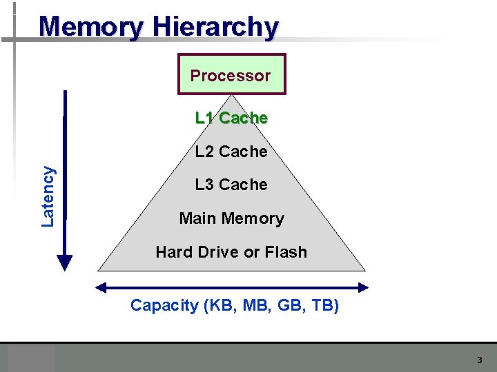
Memory Hierarchy Processor L 1 Cache Latency L 2 Cache L 3 Cache Main Memory Hard Drive or Flash Capacity (KB, MB, GB, TB) 3
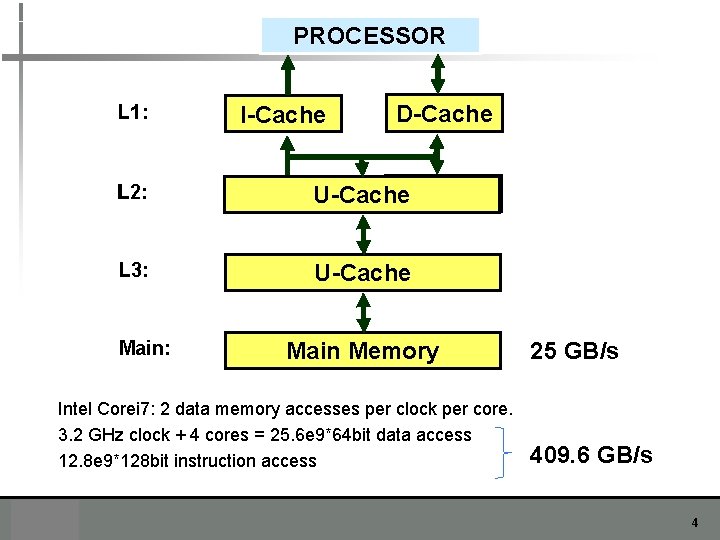
PROCESSOR D-Cache L 1: I-Cache L 2: D-Cache I-Cache U-Cache L 3: U-Cache Main: Main Memory Intel Corei 7: 2 data memory accesses per clock per core. 3. 2 GHz clock + 4 cores = 25. 6 e 9*64 bit data access 12. 8 e 9*128 bit instruction access 25 GB/s 409. 6 GB/s 4
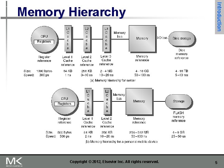
Copyright © 2012, Elsevier Inc. All rights reserved. Introduction Memory Hierarchy 5
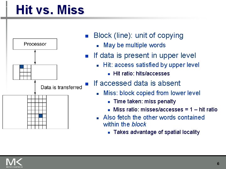
Hit vs. Miss n Block (line): unit of copying n n May be multiple words If data is present in upper level n Hit: access satisfied by upper level n n Hit ratio: hits/accesses If accessed data is absent n Miss: block copied from lower level n n n Time taken: miss penalty Miss ratio: misses/accesses = 1 – hit ratio Also fetch the other words contained within the block n Takes advantage of spatial locality 6
Tags and Valid Bits n How do we know which particular block is stored in a cache location? n n Store block address as well as the data Actually, only need the high-order bits Called the tag What if there is no data in a location? n n Valid bit: 1 = present, 0 = not present Initially 0 7
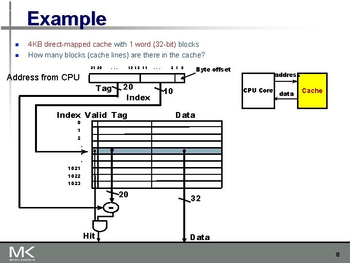
Example n n 4 KB direct-mapped cache with 1 word (32 -bit) blocks How many blocks (cache lines) are there in the cache? 31 30 . . . Address from CPU Tag 13 12 11 20 Index Valid Tag 0 . . . 2 1 0 Byte offset 10 address CPU Core data Cache Data 1 2. . . 1021 1022 1023 20 Hit 32 Data 8
Placement Policies n WHERE to put a block in cache n Mapping between main memory and cache. n Main memory has a much larger capacity than cache. 9
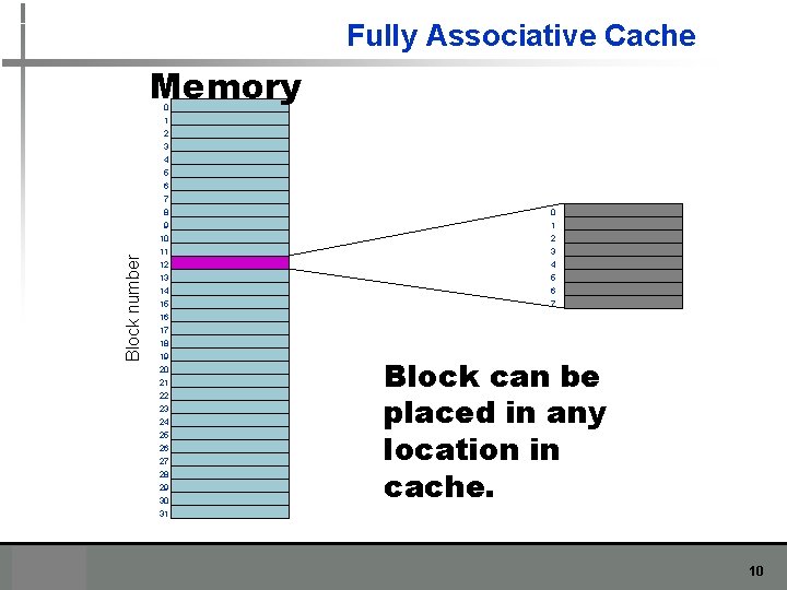
Fully Associative Cache Memory 0 1 2 3 Block number 4 5 6 7 8 9 10 11 12 13 14 15 16 17 18 19 20 21 22 23 24 25 26 27 28 29 30 31 0 1 2 3 4 5 6 7 Block can be placed in any location in cache. 10
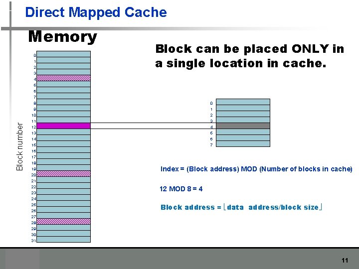
Direct Mapped Cache Memory 0 1 2 Block can be placed ONLY in a single location in cache. 3 Block number 4 5 6 7 8 9 10 11 12 13 14 15 16 17 18 19 20 21 22 23 24 25 26 27 28 29 30 31 0 1 2 3 4 5 6 7 Index = (Block address) MOD (Number of blocks in cache) 12 MOD 8 = 4 Block address = data address/block size 11
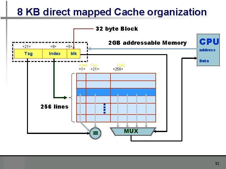
8 KB direct mapped Cache organization 32 byte Block <21> Tag <8> 2 GB addressable Memory <5> Index CPU address blk Data Valid Tag <1> <21> Data <256> : : 256 lines = MUX 12
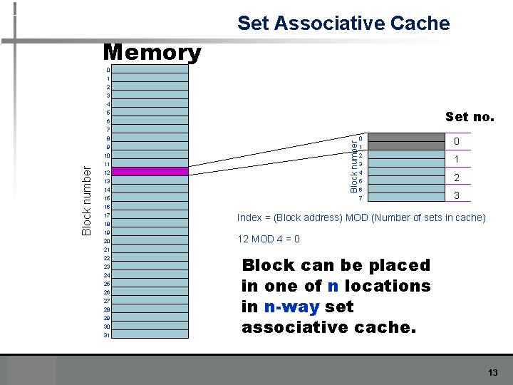
Set Associative Cache Memory 0 1 2 3 5 6 7 8 9 10 11 12 13 14 15 16 17 18 19 20 21 22 23 24 25 26 27 28 29 30 31 Set no. Block number 4 0 1 2 3 4 5 6 7 0 1 2 3 Index = (Block address) MOD (Number of sets in cache) 12 MOD 4 = 0 Block can be placed in one of n locations in n-way set associative cache. 13
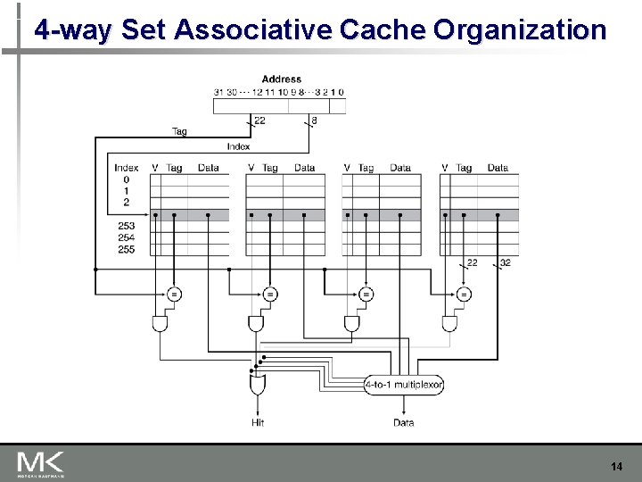
4 -way Set Associative Cache Organization 14
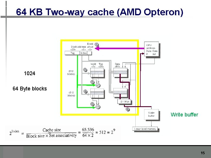
64 KB Two-way cache (AMD Opteron) 1024 64 Byte blocks Write buffer 15
Replacement Policy n n Direct mapped: no choice Set associative n n n Prefer non-valid entry, if there is one Otherwise, choose among entries in the set Least-recently used (LRU) n Choose the one unused for the longest time n n Simple for 2 -way, manageable for 4 -way, too hard beyond that Random n Gives approximately the same performance as LRU for high associativity 16
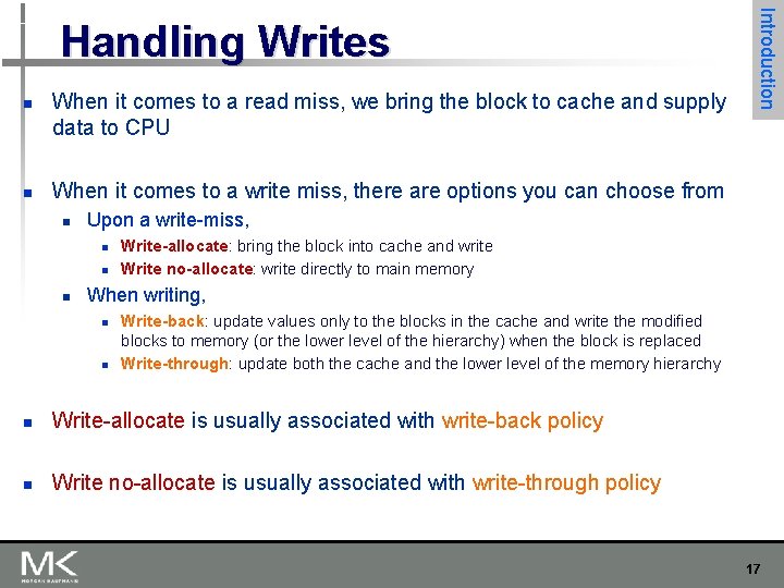
n n When it comes to a read miss, we bring the block to cache and supply data to CPU Introduction Handling Writes When it comes to a write miss, there are options you can choose from n Upon a write-miss, n n n Write-allocate: bring the block into cache and write Write no-allocate: write directly to main memory When writing, n n Write-back: update values only to the blocks in the cache and write the modified blocks to memory (or the lower level of the hierarchy) when the block is replaced Write-through: update both the cache and the lower level of the memory hierarchy n Write-allocate is usually associated with write-back policy n Write no-allocate is usually associated with write-through policy 17
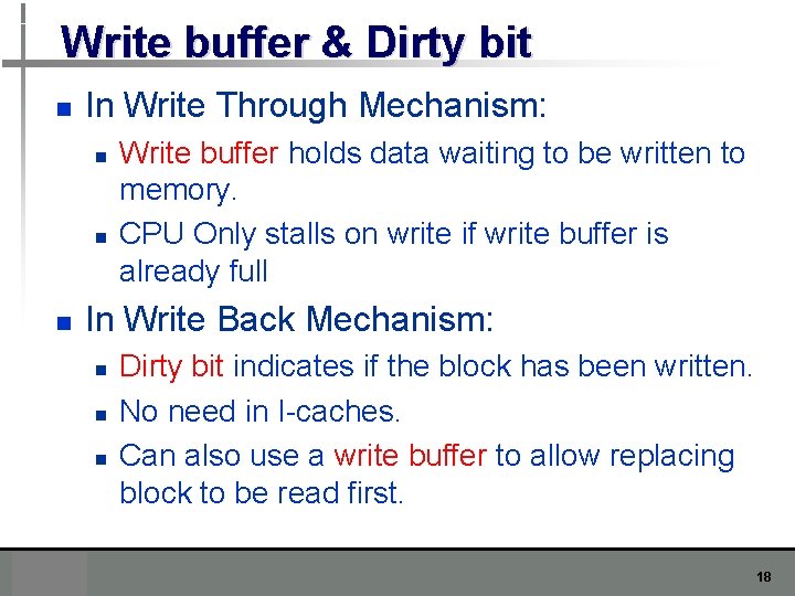
Write buffer & Dirty bit n In Write Through Mechanism: n n n Write buffer holds data waiting to be written to memory. CPU Only stalls on write if write buffer is already full In Write Back Mechanism: n n n Dirty bit indicates if the block has been written. No need in I-caches. Can also use a write buffer to allow replacing block to be read first. 18
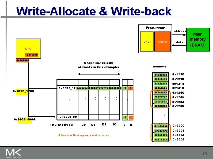
Write-Allocate & Write-back Processor CPU Cache address data CPU Main memory (DRAM) 12345678 dddd Cache line (block) (4 words in this example) memory 3434 0 x 0000_1208 0 x 0000_12 6666 77778888 5555 1 1 . . 2323 0 x 1218 1212 9999 0 x 1214 0 x 1210 8888 0 x 120 C 7777 0 x 1208 6666 0 x 1204 0 x 1200 5555 0 x 0000_00 TAG (Address) D 0 D 1 D 2 Allocate first upon a write miss D 3 1 1 V D . . . 0 x 0000_0004 0 x 121 C 4444 0 x 000 C 3333 0 x 0008 2222 0 x 0004 0 x 0000 1111 19
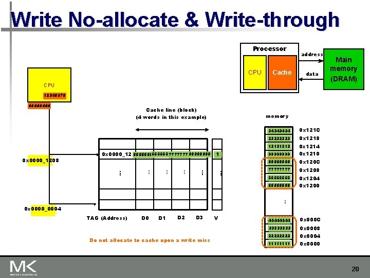
Write No-allocate & Write-through Processor CPU Cache address data CPU Main memory (DRAM) 12345678 dddd Cache line (block) (4 words in this example) memory 3434 0 x 0000_1208 0 x 0000_12 6666 77778888 5555 1 0 x 121 C . . . . 2323 0 x 1218 1212 9999 0 x 1214 0 x 1210 8888 0 x 120 C 7777 0 x 1208 6666 0 x 1204 0 x 1200 5555 . . . 0 x 0000_0004 TAG (Address) D 0 D 1 D 2 D 3 Do not allocate to cache upon a write miss V 4444 0 x 000 C 3333 0 x 0008 2222 0 x 0004 0 x 0000 1111 20
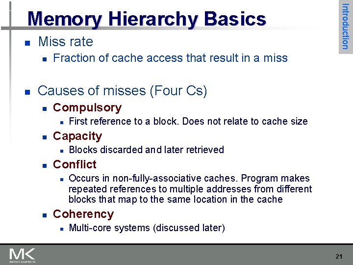
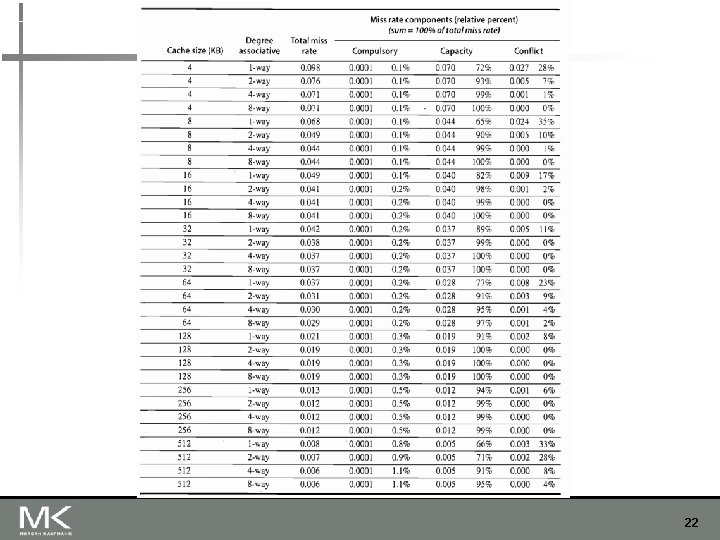
n Miss rate n n Introduction Memory Hierarchy Basics Fraction of cache access that result in a miss Causes of misses (Four Cs) n Compulsory n n Capacity n n Blocks discarded and later retrieved Conflict n n First reference to a block. Does not relate to cache size Occurs in non-fully-associative caches. Program makes repeated references to multiple addresses from different blocks that map to the same location in the cache Coherency n Multi-core systems (discussed later) 21
22
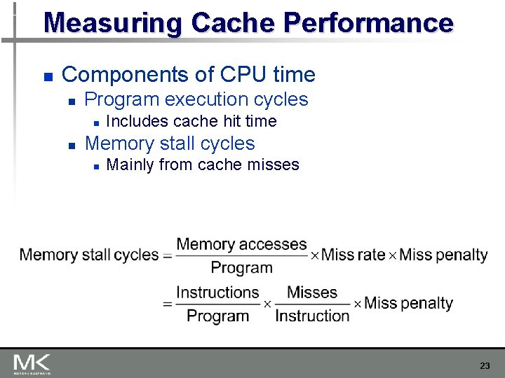
Measuring Cache Performance n Components of CPU time n Program execution cycles n n Includes cache hit time Memory stall cycles n Mainly from cache misses 23
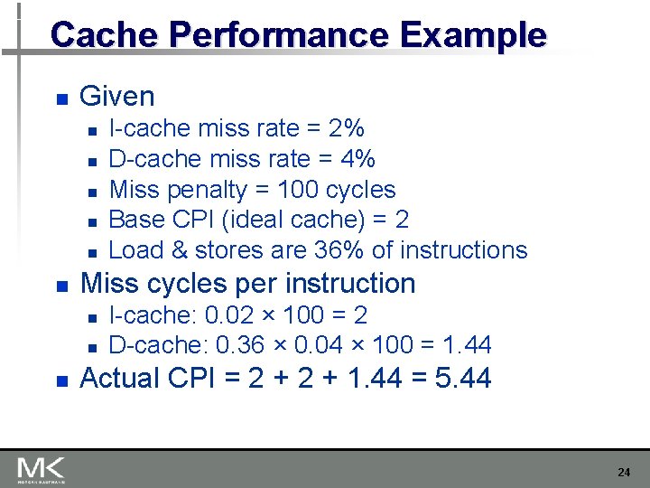
Cache Performance Example n Given n n n Miss cycles per instruction n I-cache miss rate = 2% D-cache miss rate = 4% Miss penalty = 100 cycles Base CPI (ideal cache) = 2 Load & stores are 36% of instructions I-cache: 0. 02 × 100 = 2 D-cache: 0. 36 × 0. 04 × 100 = 1. 44 Actual CPI = 2 + 1. 44 = 5. 44 24
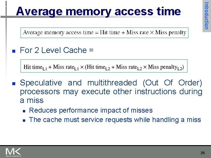
Introduction Average memory access time n n For 2 Level Cache = Speculative and multithreaded (Out Of Order) processors may execute other instructions during a miss n n Reduces performance impact of misses The cache must service requests while handling a miss 25
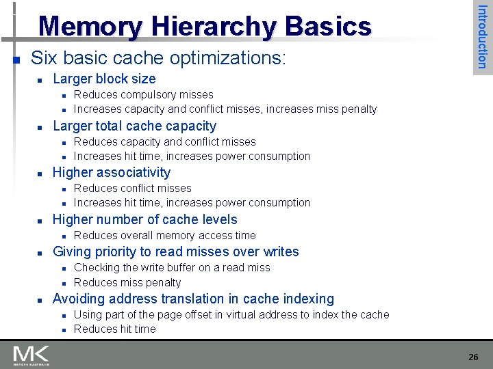
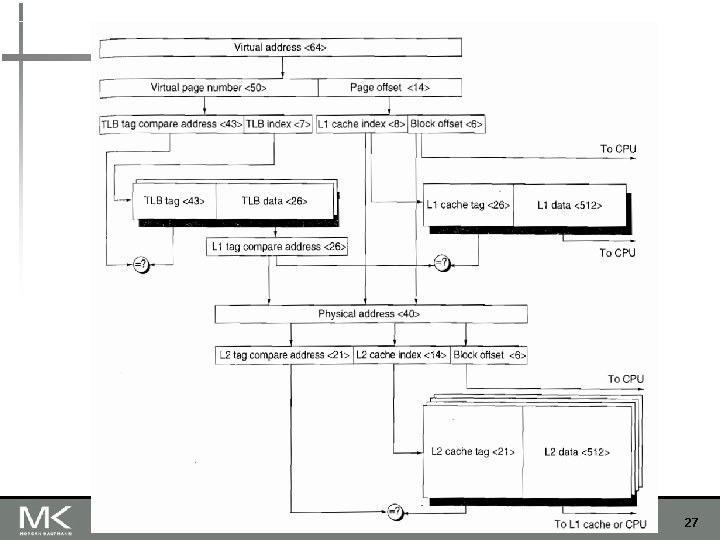
n Six basic cache optimizations: n Larger block size n n n Reduces overall memory access time Giving priority to read misses over writes n n n Reduces conflict misses Increases hit time, increases power consumption Higher number of cache levels n n Reduces capacity and conflict misses Increases hit time, increases power consumption Higher associativity n n Reduces compulsory misses Increases capacity and conflict misses, increases miss penalty Larger total cache capacity n n Introduction Memory Hierarchy Basics Checking the write buffer on a read miss Reduces miss penalty Avoiding address translation in cache indexing n n Using part of the page offset in virtual address to index the cache Reduces hit time 26
Copyright © 2012, Elsevier Inc. All rights reserved. 27
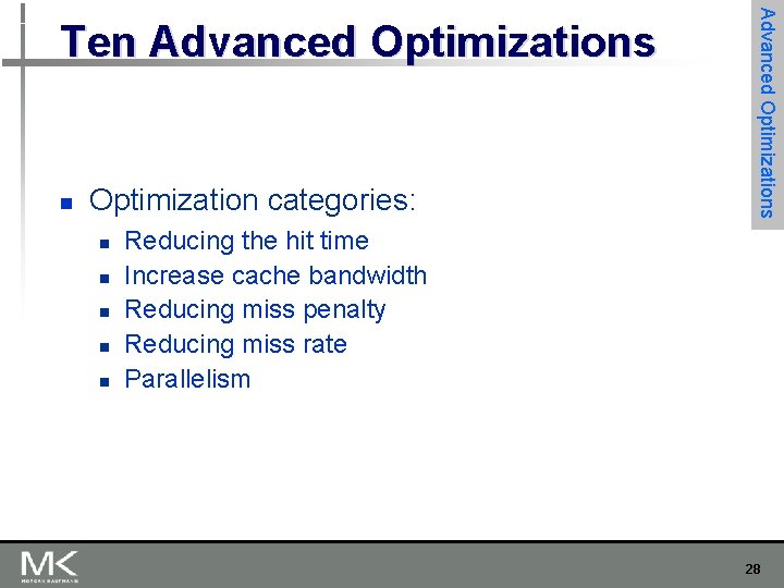
n Optimization categories: n n n Advanced Optimizations Ten Advanced Optimizations Reducing the hit time Increase cache bandwidth Reducing miss penalty Reducing miss rate Parallelism 28
1) Small and simple L 1 caches n n n Limited size and lower associativity results lower hit time. Critical timing path: n addressing tag memory using the index n comparing read tags with address n selecting correct word by multiplexing the offset Lower associativity reduces power because fewer cache lines are accessed - Not direct mapped because: n Virtual indexing needs the cache size to be the page size times the associativity n Multi-threading increase conflict misses in lower associativities. 29
n To improve hit time, predict the way n Uses predictor bits in each cache line for next access prediction. n Prediction accuracy n > 90% for two-way n > 80% for four-way n I-cache has better prediction accuracy than D-cache n First used on MIPS R 10000 in mid-90 s n Used on 4 -way caches in ARM Cortex-A 8 n decreases energy by 0. 28 in I-cache and 0. 35 in D-cache n Advanced Optimizations 2) Way Prediction Increases mis-prediction penalty and average access time to 1. 04 in I-cache and 1. 13 in D-cache. 30
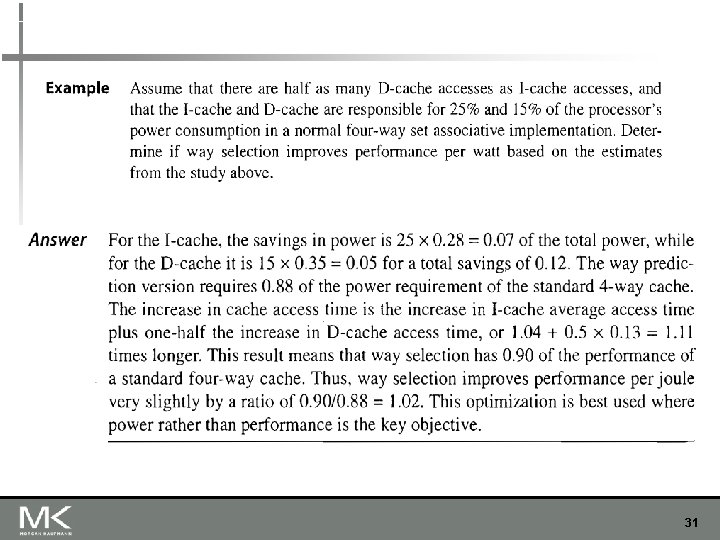
31
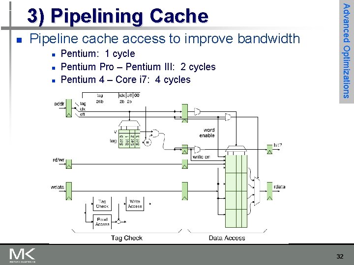
n Pipeline cache access to improve bandwidth n n n Pentium: 1 cycle Pentium Pro – Pentium III: 2 cycles Pentium 4 – Core i 7: 4 cycles Advanced Optimizations 3) Pipelining Cache 32
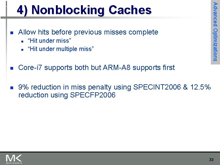
Advanced Optimizations 4) Nonblocking Caches n Allow hits before previous misses complete n n "Hit under miss" "Hit under multiple miss" Core-i 7 supports both but ARM-A 8 supports first 9% reduction in miss penalty using SPECINT 2006 & 12. 5% reduction using SPECFP 2006 33
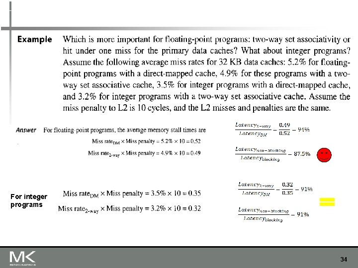
For integer programs 34
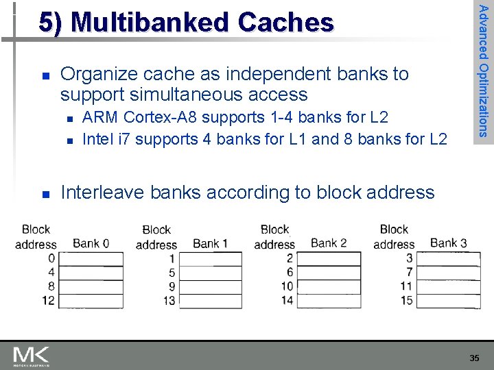
n Organize cache as independent banks to support simultaneous access n n n ARM Cortex-A 8 supports 1 -4 banks for L 2 Intel i 7 supports 4 banks for L 1 and 8 banks for L 2 Advanced Optimizations 5) Multibanked Caches Interleave banks according to block address 35
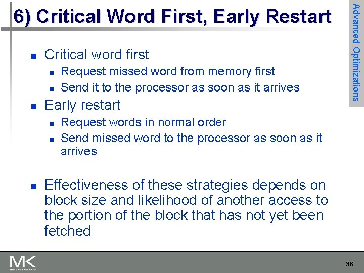
n Critical word first n n n Early restart n n n Request missed word from memory first Send it to the processor as soon as it arrives Advanced Optimizations 6) Critical Word First, Early Restart Request words in normal order Send missed word to the processor as soon as it arrives Effectiveness of these strategies depends on block size and likelihood of another access to the portion of the block that has not yet been fetched 36
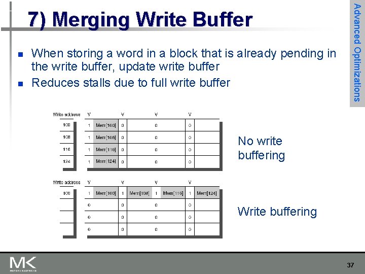
n n When storing a word in a block that is already pending in the write buffer, update write buffer Reduces stalls due to full write buffer Advanced Optimizations 7) Merging Write Buffer No write buffering Write buffering 37
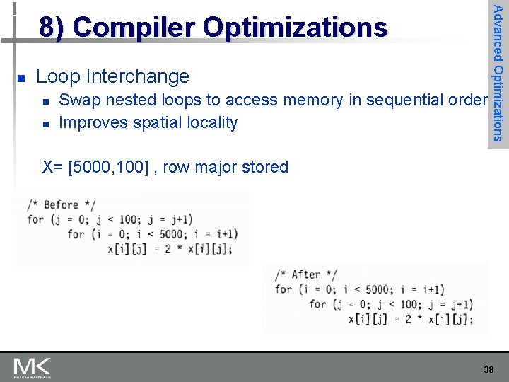
n Loop Interchange n n Swap nested loops to access memory in sequential order Improves spatial locality Advanced Optimizations 8) Compiler Optimizations X= [5000, 100] , row major stored 38
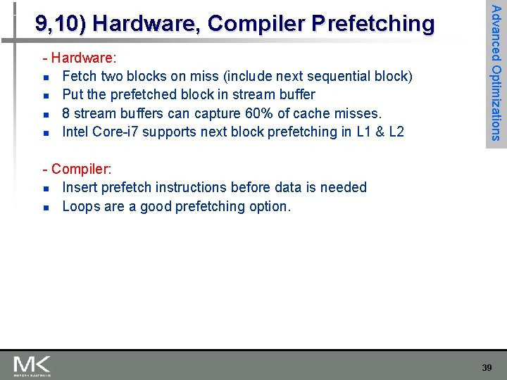
- Hardware: n Fetch two blocks on miss (include next sequential block) n Put the prefetched block in stream buffer n 8 stream buffers can capture 60% of cache misses. n Intel Core-i 7 supports next block prefetching in L 1 & L 2 Advanced Optimizations 9, 10) Hardware, Compiler Prefetching - Compiler: n Insert prefetch instructions before data is needed n Loops are a good prefetching option. 39
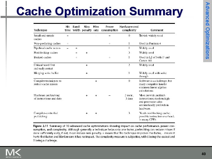
Advanced Optimizations Cache Optimization Summary 40
n Performance metrics n n Main memory Latency is primery concern of cache Bandwidth is concern of multiprocessors and I/O With increased block size, main memory bandwidth is also important to caches Access time n n n Time between read request and when desired word arrives Cycle time n n Memory Technology Minimum time between unrelated requests to memory DRAM used for main memory, SRAM used for cache Flash memory for PMDs. 41
n SRAM n n n Access time is close to cycle time Requires low power to retain bit Requires 6 transistors/bit Largest L 3 SRAM = 12 MB 4 times faster than DRAM Memory Technology DRAM n n n Must be re-written after being read Cycle time is longer than the access time Must also be periodically refreshed n Every ~ 8 ms : takes 5% of memory time n Each row can be refreshed simultaneously One transistor/bit Address lines are multiplexed due to large size: n Upper half of address: row access strobe (RAS) n Lower half of address: column access strobe (CAS) 42
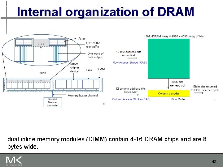
Internal organization of DRAM dual inline memory modules (DIMM) contain 4 -16 DRAM chips and are 8 bytes wide. 43
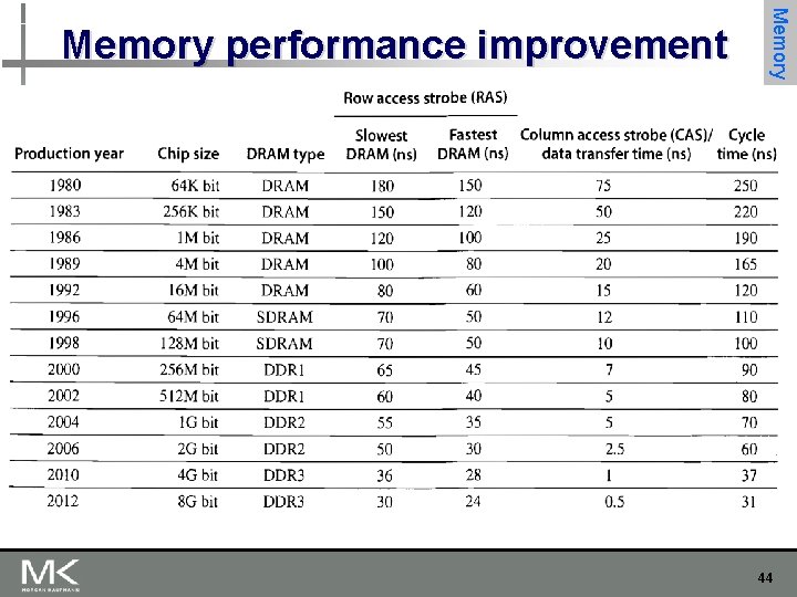
Memory Technology Memory performance improvement 44
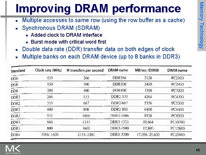
n n Multiple accesses to same row (using the row buffer as a cache) Synchronous DRAM (SDRAM) n n Added clock to DRAM interface Burst mode with critical word first Double data rate (DDR) transfer data on both edges of clock Multiple banks on each DRAM device (up to 8 banks in DDR 3) Memory Technology Improving DRAM performance 45
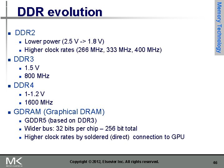
n DDR 2 n n n DDR 3 n n n 1. 5 V 800 MHz DDR 4 n n n Lower power (2. 5 V -> 1. 8 V) Higher clock rates (266 MHz, 333 MHz, 400 MHz) Memory Technology DDR evolution 1 -1. 2 V 1600 MHz GDRAM (Graphical DRAM) n n n GDDR 5 (based on DDR 3) Wider bus: 32 bits per chip – 256 bit total Higher clock rates by soldered (direct) connection to GPU Copyright © 2012, Elsevier Inc. All rights reserved. 46
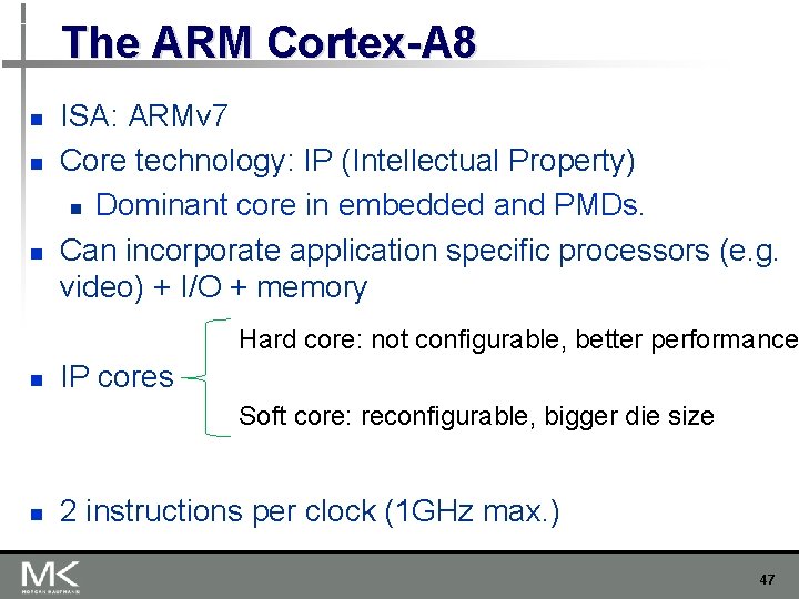
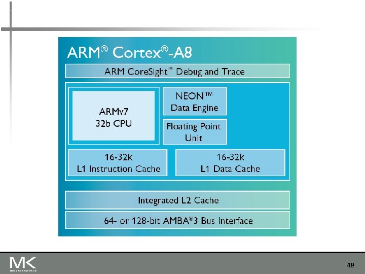
The ARM Cortex-A 8 n n n ISA: ARMv 7 Core technology: IP (Intellectual Property) n Dominant core in embedded and PMDs. Can incorporate application specific processors (e. g. video) + I/O + memory Hard core: not configurable, better performance n IP cores Soft core: reconfigurable, bigger die size n 2 instructions per clock (1 GHz max. ) 47
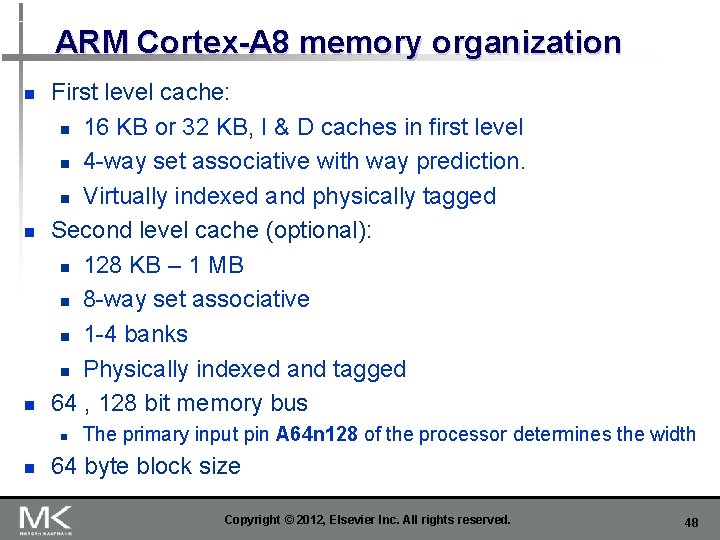
ARM Cortex-A 8 memory organization n First level cache: n 16 KB or 32 KB, I & D caches in first level n 4 -way set associative with way prediction. n Virtually indexed and physically tagged Second level cache (optional): n 128 KB – 1 MB n 8 -way set associative n 1 -4 banks n Physically indexed and tagged 64 , 128 bit memory bus n n The primary input pin A 64 n 128 of the processor determines the width 64 byte block size Copyright © 2012, Elsevier Inc. All rights reserved. 48
49
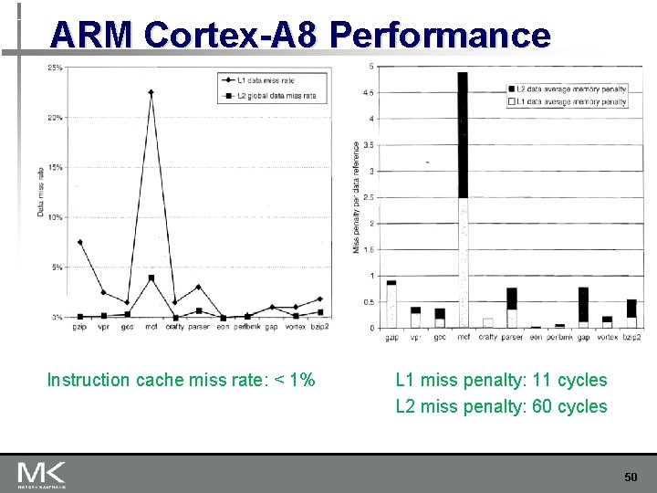
ARM Cortex-A 8 Performance Instruction cache miss rate: < 1% L 1 miss penalty: 11 cycles L 2 miss penalty: 60 cycles 50
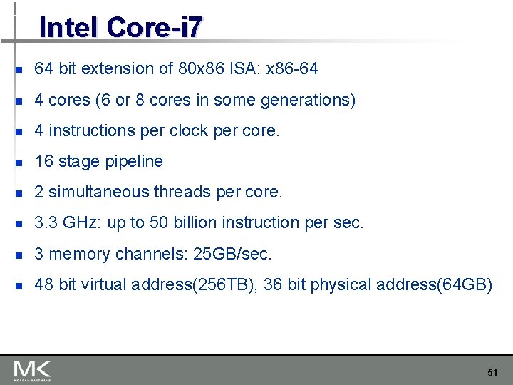
Intel Core-i 7 n 64 bit extension of 80 x 86 ISA: x 86 -64 n 4 cores (6 or 8 cores in some generations) n 4 instructions per clock per core. n 16 stage pipeline n 2 simultaneous threads per core. n 3. 3 GHz: up to 50 billion instruction per sec. n 3 memory channels: 25 GB/sec. n 48 bit virtual address(256 TB), 36 bit physical address(64 GB) 51
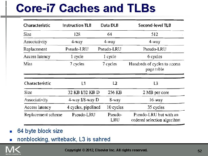
Core-i 7 Caches and TLBs n n 64 byte block size nonblocking, writeback, L 3 is sahred Copyright © 2012, Elsevier Inc. All rights reserved. 52
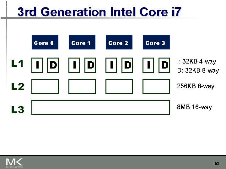
3 rd Generation Intel Core i 7 Core 0 L 1 I D Core 2 I D Core 3 I D I: 32 KB 4 -way D: 32 KB 8 -way L 2 256 KB 8 -way L 3 8 MB 16 -way 53
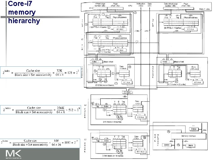
Core-i 7 memory hierarchy 54
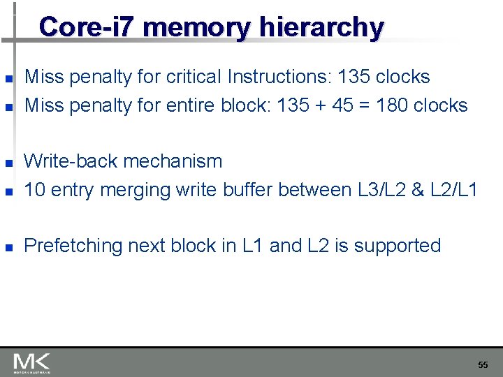
Core-i 7 memory hierarchy n n Miss penalty for critical Instructions: 135 clocks Miss penalty for entire block: 135 + 45 = 180 clocks n Write-back mechanism 10 entry merging write buffer between L 3/L 2 & L 2/L 1 n Prefetching next block in L 1 and L 2 is supported n 55
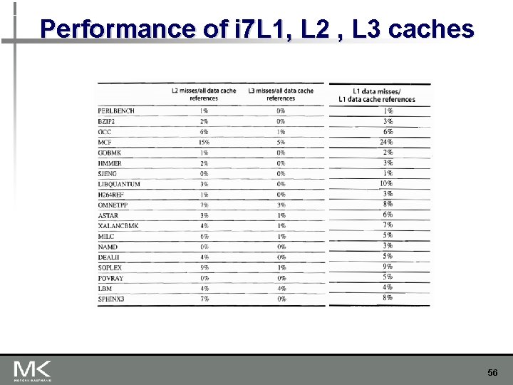
Performance of i 7 L 1, L 2 , L 3 caches 56
Computer Architecture a Quantitative Approach Fifth Edition Chapter 2 Solutions
Source: https://slidetodoc.com/computer-architecture-a-quantitative-approach-fifth-edition-chapter/